
1.
General description
The 74HC4053; 74HCT4053 is a high-speed Si-gate CMOS device and is pin compatible
with the HEF4053B. It is specified in compliance with JEDEC standard no. 7A.
The 74HC4053; 74HCT4053 is triple 2-channel analog multiplexer/demultiplexer with a
common enable input (E). Each multiplexer/demultiplexer has two independent
inputs/outputs (nY0 and nY1), a common input/output (nZ) and three digital select
inputs (Sn).
With E LOW, one of the two switches is selected (low-impedance ON-state) by S1 to S3.
With E HIGH, all switches are in the high-impedance OFF-state, independent of S1 to S3.
V
CC
and GND are the supply voltage pins for the digital control inputs (S1 to S3 and E).
The V
CC
to GND ranges are 2.0 V to 10.0 V for 74HC4053 and 4.5 V to 5.5 V for
74HCT4053. The analog inputs/outputs (nY0 and nY1, and nZ) can swing between V
CC
as a positive limit and V
EE
as a negative limit. V
CC
-
V
EE
may not exceed 10.0 V.
For operation as a digital multiplexer/demultiplexer, V
EE
is connected to GND (typically
ground).
2.
Features
s
Low ON resistance:
x
80
(typical) at V
CC
-
V
EE
= 4.5 V
x
70
(typical) at V
CC
-
V
EE
= 6.0 V
x
60
(typical) at V
CC
-
V
EE
= 9.0 V
s
Logic level translation:
x
To enable 5 V logic to communicate with
�
5 V analog signals
s
Typical `break before make' built in
s
Complies with JEDEC standard no. 7A
s
ESD protection:
x
HBM EIA/JESD22-A114-C exceeds 2000 V
x
MM EIA/JESD22-A115-A exceeds 200 V
s
Multiple package options
s
Specified from
-
40
�
C to +85
�
C and from
-
40
�
C to +125
�
C
74HC4053; 74HCT4053
Triple 2-channel analog multiplexer/demultiplexer
Rev. 04 -- 9 May 2006
Product data sheet

74HC_HCT4053_4
� Koninklijke Philips Electronics N.V. 2006. All rights reserved.
Product data sheet
Rev. 04 -- 9 May 2006
2 of 33
Philips Semiconductors
74HC4053; 74HCT4053
Triple 2-channel analog multiplexer/demultiplexer
3.
Applications
s
Analog multiplexing and demultiplexing
s
Digital multiplexing and demultiplexing
s
Signal gating
4.
Quick reference data
[1]
C
PD
is used to determine the dynamic power dissipation (P
D
in
�
W).
P
D
= C
PD
�
V
CC
2
�
f
i
+
{(C
L
+ C
S
)
�
V
CC
2
�
f
o
} where:
f
i
= input frequency in MHz;
f
o
= output frequency in MHz;
{(C
L
+ C
S
)
�
V
CC
2
�
f
o
} = sum of outputs;
Table 1:
Quick reference data
V
EE
= GND = 0 V; T
amb
= 25
�
C; t
r
= t
f
= 6 ns.
Symbol Parameter
Conditions
Min
Typ
Max
Unit
74HC4053
t
PZH
,
t
PZL
turn-ON time
C
L
= 15 pF; R
L
= 1 k
;
V
CC
= 5 V
E to V
os
-
17
-
ns
Sn to V
os
-
21
-
ns
t
PHZ
,
t
PLZ
turn-OFF time
C
L
= 15 pF; R
L
= 1 k
;
V
CC
= 5 V
E to V
os
-
18
-
ns
Sn to V
os
-
17
-
ns
C
i
input capacitance
-
3.5
-
pF
C
S
switch capacitance
independent I/O (nYn)
-
5
-
pF
common I/O (nZ)
-
8
-
pF
C
PD
power dissipation
capacitance
per switch; V
I
= GND to
V
CC
[1]
-
36
-
pF
74HCT4053
t
PZH
,
t
PZL
turn-ON time
C
L
= 15 pF; R
L
= 1 k
;
V
CC
= 5 V
E to V
os
-
23
-
ns
Sn to V
os
-
21
-
ns
t
PHZ
,
t
PLZ
turn-OFF time
C
L
= 15 pF; R
L
= 1 k
;
V
CC
= 5 V
E to V
os
-
20
-
ns
Sn to V
os
-
19
-
ns
C
i
input capacitance
-
3.5
-
pF
C
S
switch capacitance
independent I/O (nYn)
-
5
-
pF
common I/O(nZ)
-
8
-
pF
C
PD
power dissipation
capacitance
per switch; V
I
= GND to
(V
CC
-
1.5 V)
[1]
-
36
-
pF

74HC_HCT4053_4
� Koninklijke Philips Electronics N.V. 2006. All rights reserved.
Product data sheet
Rev. 04 -- 9 May 2006
3 of 33
Philips Semiconductors
74HC4053; 74HCT4053
Triple 2-channel analog multiplexer/demultiplexer
C
L
= output load capacitance in pF;
C
S
= maximum switch capacitance in pF;
V
CC
= supply voltage in V.
5.
Ordering information
Table 2:
Ordering information
Type number
Package
Temperature range
Name
Description
Version
74HC4053
74HC4053N
-
40
�
C to +125
�
C
DIP16
plastic dual in-line package; 16 leads (300 mil); long
body
SOT38-4
74HC4053D
-
40
�
C to +125
�
C
SO16
plastic small outline package; 16 leads; body width
3.9 mm
SOT109-1
74HC4053DB
-
40
�
C to +125
�
C
SSOP16
plastic shrink small outline package; 16 leads; body
width 5.3 mm
SOT338-1
74HC4053PW
-
40
�
C to +125
�
C
TSSOP16
plastic thin shrink small outline package; 16 leads;
body width 4.4 mm
SOT403-1
74HC4053BQ
-
40
�
C to +125
�
C
DHVQFN16 plastic dual in-line compatible thermal enhanced very
thin quad flat package; no leads; 16 terminals;
body 2.5
�
3.5
�
0.85 mm
SOT763-1
74HCT4053
74HCT4053N
-
40
�
C to +125
�
C
DIP16
plastic dual in-line package; 16 leads (300 mil); long
body
SOT38-4
74HCT4053D
-
40
�
C to +125
�
C
SO16
plastic small outline package; 16 leads; body width
3.9 mm
SOT109-1
74HCT4053DB
-
40
�
C to +125
�
C
SSOP16
plastic shrink small outline package; 16 leads; body
width 5.3 mm
SOT338-1
74HCT4053PW
-
40
�
C to +125
�
C
TSSOP16
plastic thin shrink small outline package; 16 leads;
body width 4.4 mm
SOT403-1
74HCT4053BQ
-
40
�
C to +125
�
C
DHVQFN16 plastic dual in-line compatible thermal enhanced very
thin quad flat package; no leads; 16 terminals;
body 2.5
�
3.5
�
0.85 mm
SOT763-1
74HC_HCT4053_4
� Koninklijke Philips Electronics N.V. 2006. All rights reserved.
Product data sheet
Rev. 04 -- 9 May 2006
4 of 33
Philips Semiconductors
74HC4053; 74HCT4053
Triple 2-channel analog multiplexer/demultiplexer
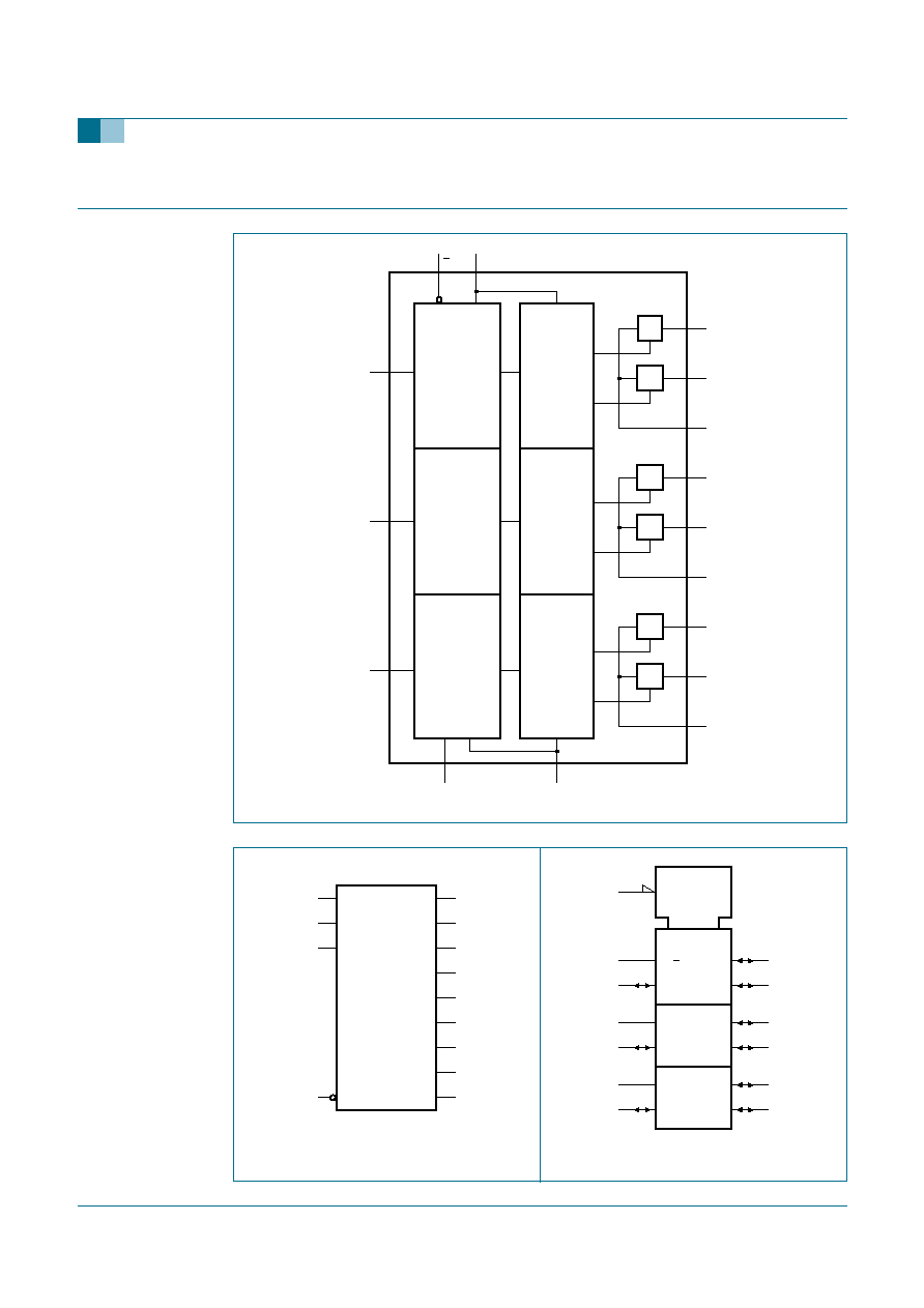
6.
Functional diagram
Fig 1.
Functional diagram
Fig 2.
Logic symbol
Fig 3.
IEC logic symbol
001aae124
LOGIC
LEVEL
CONVERSION
11
16
V
CC
13 1Y1
S1
DECODER
12 1Y0
14 1Z
1 2Y1
2 2Y0
15 2Z
3 3Y1
5 3Y0
4 3Z
10
S2
9
8
7
GND
V
EE
S3
6
E
001aae125
1Y0
12
1Y1
S1
13
11
S2
10
S3
9
6
E
2Y0
2
2Y1
1
3Y0
5
3Y1
3
3Z
4
2Z
15
1Z
14
001aae126
6
EN
11
#
#
#
MUX/DMUX
12
13
�
0
1
0/1
0
1
14
10
2
1
15
9
5
3
4

74HC_HCT4053_4
� Koninklijke Philips Electronics N.V. 2006. All rights reserved.
Product data sheet
Rev. 04 -- 9 May 2006
5 of 33
Philips Semiconductors
74HC4053; 74HCT4053
Triple 2-channel analog multiplexer/demultiplexer
7.
Pinning information
7.1 Pinning
Fig 4.
Schematic diagram (one switch)
001aad544
from
logic
V
CC
V
EE
V
EE
V
CC
V
CC
V
EE
Y
Z
V
CC
(1) The die substrate is attached to this
pad using conductive die attach
material. It can not be used as supply
pin or input.
Fig 5.
Pin configuration DIP16, SO16 and
(T)SSOP16
Fig 6.
Pin configuration DHVQFN16
74HC4053
74HCT4053
2Y1
V
CC
2Y0
2Z
3Y1
1Z
3Z
1Y1
3Y0
1Y0
E
S1
V
EE
S2
GND
S3
001aae127
1
2
3
4
5
6
7
8
10
9
12
11
14
13
16
15
001aae128
V
EE
S2
E
S1
3Y0
1Y0
3Z
1Y1
3Y1
1Z
2Y0
2Z
GND
S3
2Y1
V
CC
Transparent top view
7
10
6
11
5
12
4
13
3
14
2
15
8
9
1
16
terminal 1
index area
GND
(1)
74HC4053
74HCT4053